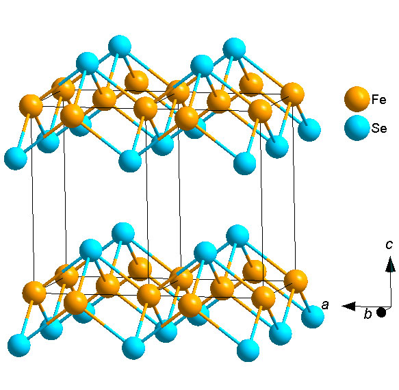
Figure 1. Crystal structure of FeSe.
FeSe-based superconductors have the simplest chemical composition and lattice structure in iron based superconductors,but have the most abundant physical properties. Its transition temperature can be tuned widely using various means, and it is an ideal object for studying iron based superconductivity. Our group can grow high quality FeSe thin films, and can tune the superconductivity and lattice structure of thin films by various means.
Uniform FeSe films on 12 kinds of substrates
We have grown FeSe single crystal thin films on 12 different substrates, and all these films have very high epitaxiality and good crystal quality [1]
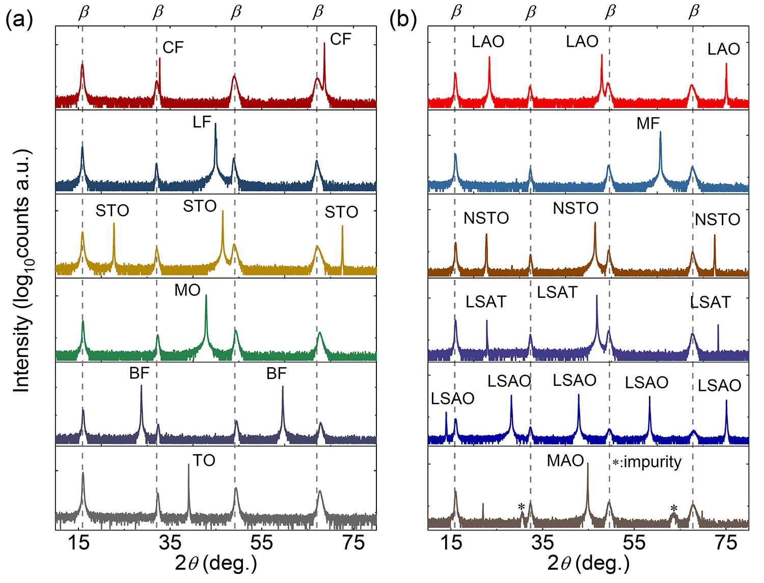
Figure 2-13 XRD θ-2θ Scan data of FeSe thin films on different substrates
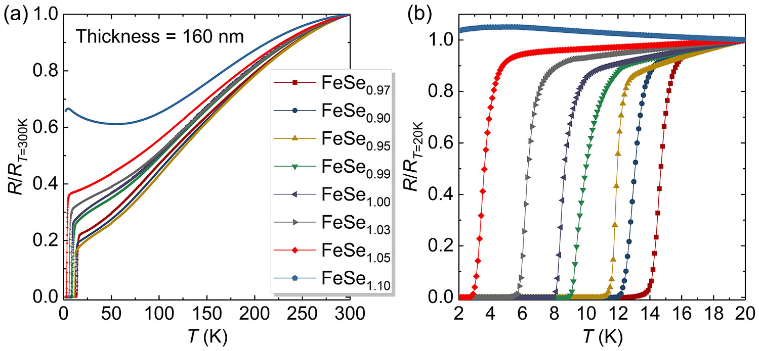
Figure 2-14 R-T data of FeSe thin films on different substrates
High epitaxial quality and crystal quality
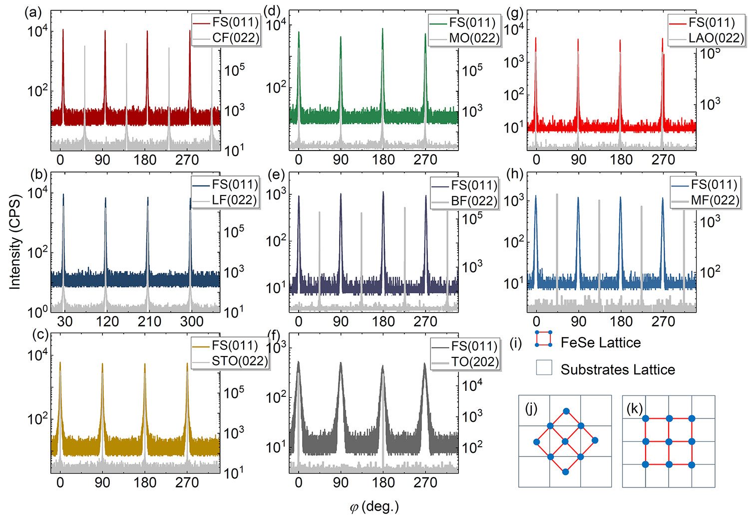
Figure 2-16 XRD φ Scan data of FeSe thin films on different substrates and Schematic diagram of epitaxial matching
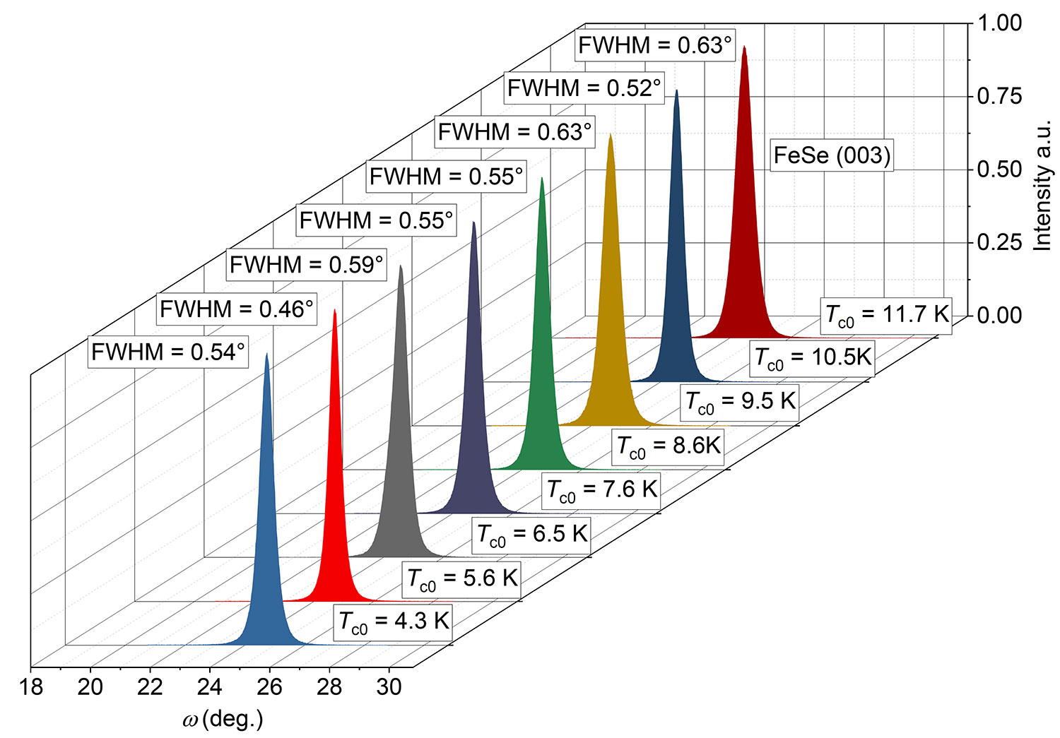
Figure 2-17 Rocking curve of FeSe thin films on different substrates
High quality FeSe thin film with a thickness of 20nm
As the thickness of the film decreases, the proportion of impurities and dead layers in the film increases, which will affect the superconductivity of the film. However, in the samples grown by our group, even if the film thickness is reduced to 20nm, it still has a high flatness and good superconductivity, indicating that our samples have a thin dead layer and few impurities [2]。

Figure 2-18 Experimental data of three film thickness characterization experiments of the 20 nm FeSe thin film (a) is the Laue oscillation curve of the FeSe (001) peak of the thin film sample; Figure (b) is the data of X-ray reflectance. Combined, the film thickness and surface roughness can be obtained as h = 20±1 nm and r ~ 0.8 nm respectively; Figure (c) is the SEM image of the sample cross section。
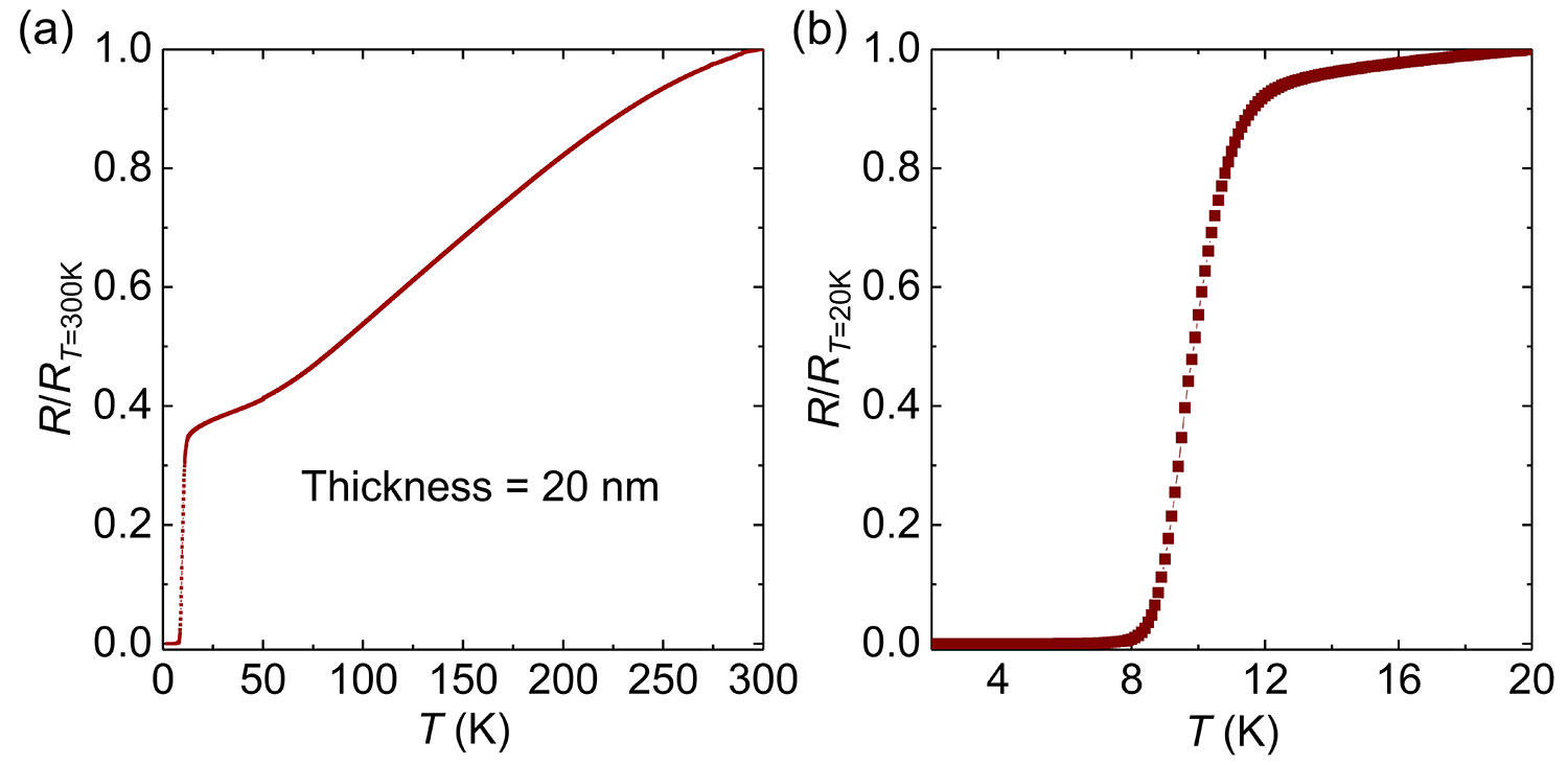
Figure 2-22 R-T data of 20 nm FeSe/LiF thin film, indicating the dead layer is thin
FeSe thin film samples of various nominal stoichiometry targets
A slight change in the ratio of Fe to Se in the FeSe material will changes the FeSe superconductivity. Using targets with different stoichiometry, we can also realize the regulation of the superconductivity of the FeSe thin film [1].

Figure 2-23 R-T data of FeSe/CaF2 thin films of different targets Except for the samples prepared with Fe:Se = 1:1.10 target, which exhibited semiconductor behavior, the other samples all exhibited metal resistance characteristics. Data is derived from the sample with the highest Tc in each target.
Large-scale regulation of FeSe thin film superconductivity using the same target
Even for a target with a single nominal stoichiometry, we can still achieve a wide range of Tc control of FeSe thin films on the same substrate by changing the growth conditions. Taking the CaF2 substrate as an example, we have achieved FeSe samples from 4.3K to 11.7K .And the different batches of grown films all have good crystallinity.
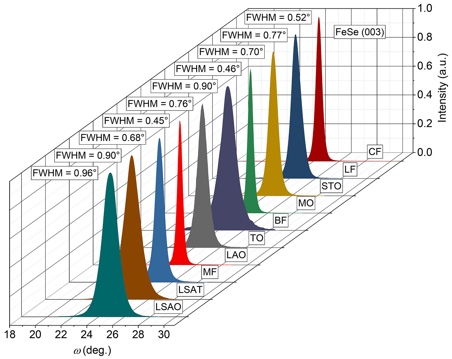
Figure 2-28 Rocking curve of different preparation batches of FeSe/CaF2 thin film
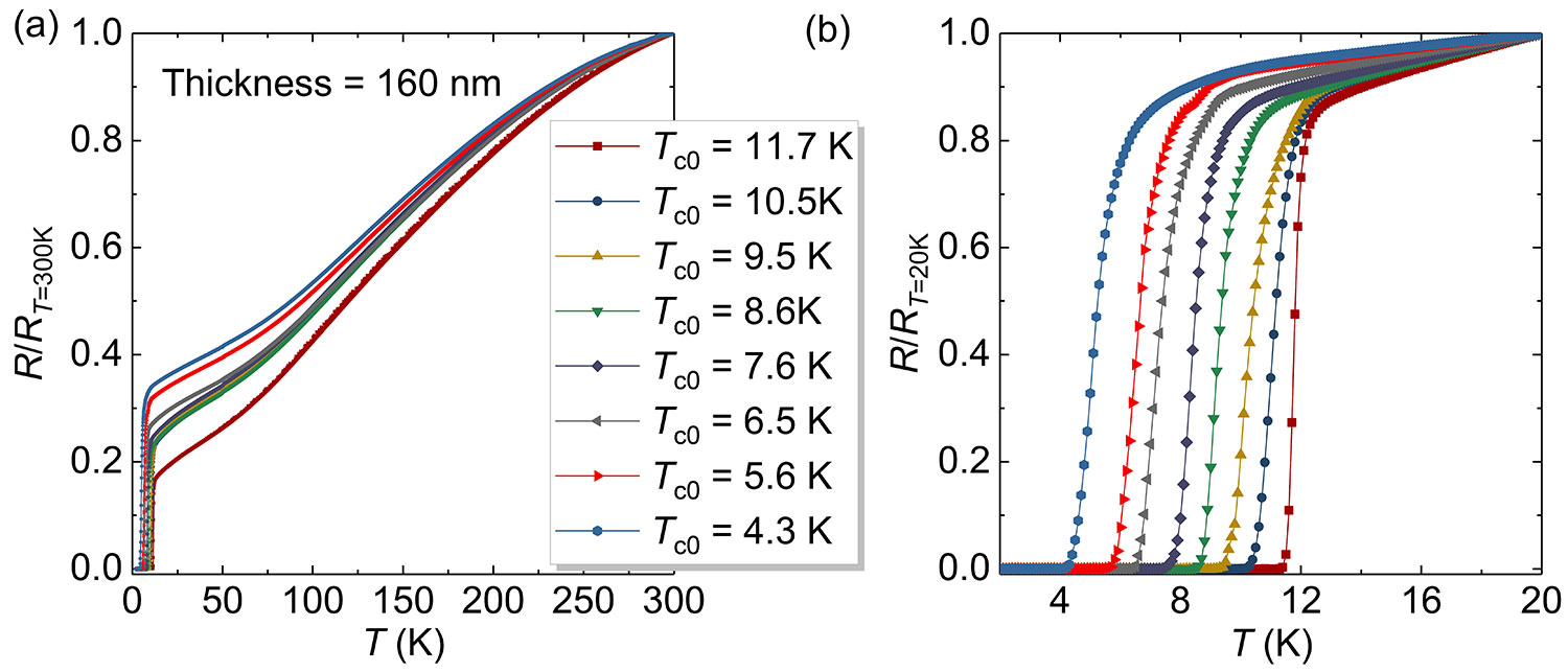
Figure 2-26 R-T data of different batches of FeSe/CaF2 films The above samples all use the same FeSe0.90 target and CaF2 substrate, and the film thickness is controlled to 160 nm.
Quality optimization and screening of FeSe thin film samples
Based on the growth and characterization of 1500 samples [2], we have continuously optimized the preparation process of FeSe thin films, and the minimum superconducting transition width of FeSe thin films can reach 0.3K. Through the optimization of the preparation process, we can achieve fine control of the properties of the FeSe thin film.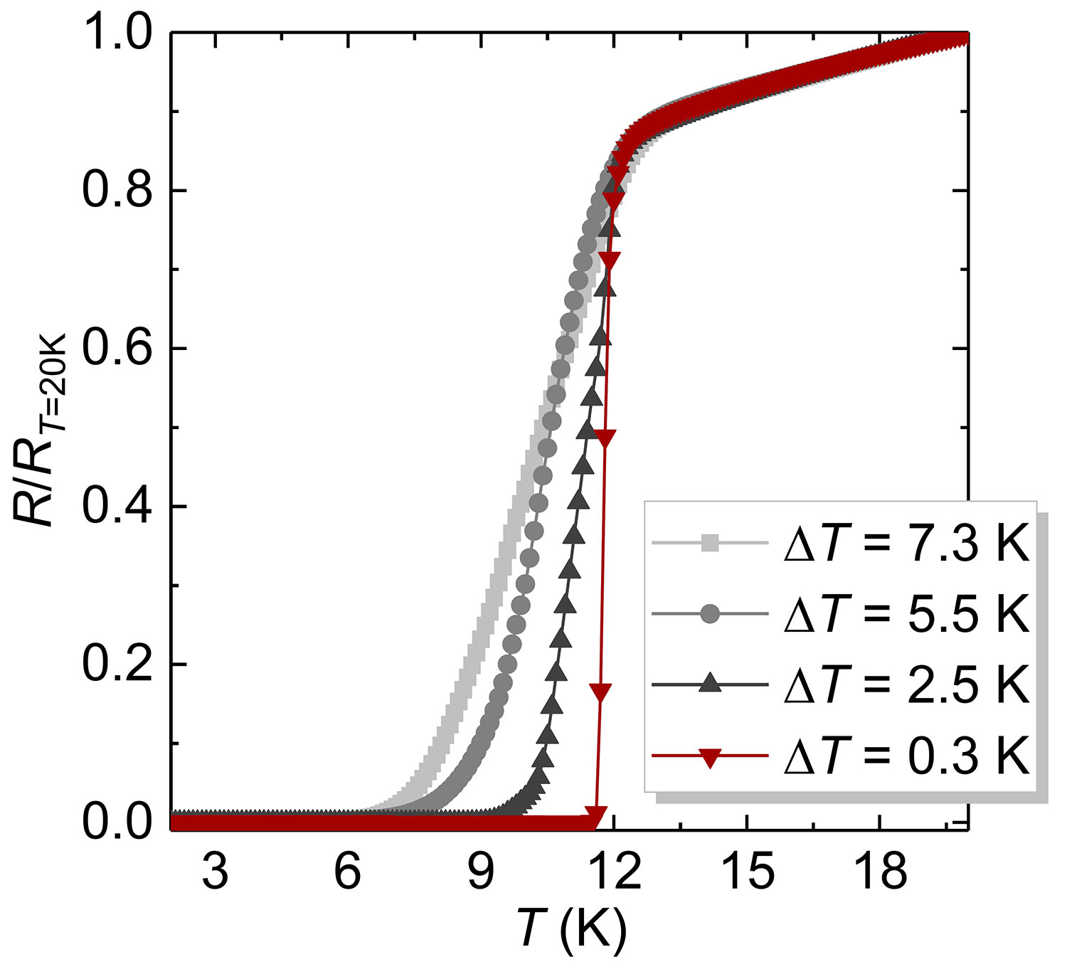
Figure 2-30 R-T data of FeSe/CaF2 films with different uniformity by continuous optimization of the preparation process, the minimum superconducting transition width of FeSe thin film can reach 0.3 K.
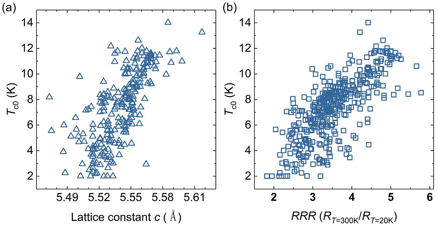
Figure 2-31 The relationship between the superconductivity of FeSe thin film and its lattice constant c and RRR
Based on the deposition and characterization of more than 1500 samples, in order to achieve the quality optimization and screening of thin film samples
Surface flatness, stripping and transfer of thin films
Our film has a high surface smoothness, and can be stripping and transferred, which is beneficial to STM, ARPES and other means of measurement.

Figure 2-33 SEM images of surface morphology of different FeSe/CaF2 thin film samples; There are spherical precipitates with a diameter of about 50 nm on the surface of the film, which is a common feature of PLD films.
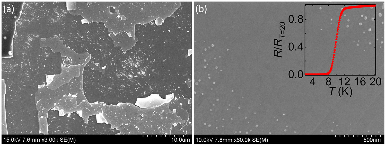
Figure 2-34 SEM image and R-T data after FeSe thin film after stripping Figure (a) is the step morphology of the surface of the FeSe film left on the substrate after the film sample stripped; Figure (b) is the surface of the stripped surface of the FeSe sheet part of the film surface after the sample is stripped and transferred Enlarged view of the morphology, the upper right illustration is the RT data of the FeSe sheet obtained by stripping and transfer.
More
 Zhongpei Feng, Jie Yuan, Ge He, Wei Hu, Zefeng Lin, Dong Li, Xingyu Jiang, Yulong Huang, Shunli Ni, Jun Li,Beiyi Zhu, Xiaoli Dong, Fang Zhou, Huabing Wang, Zhongxian Zhao and Kui Jin, Tunable critical temperature for superconductivity in FeSe thin films by pulsed laser deposition
 Yang Hua, Feng Zhong-Pei, Lin Ze-Feng, Hu Wei, Qin Ming-Yang, Zhu Bei-Yi, Yuan Jie and Jin Kui, Preparation and characterization of high-quality FeSe single crystal thin films, Acta Phys. Sin. 67 207416 (2018)


 EN
EN